Global Circuit Solutions Inc. is a leading supplier of printed circuit boards (PCBs). With a commitment to quality, innovation, and reliability, we have firmly established ourselves as a top-tier supplier of PCB solutions. Our state-of-the-art manufacturing facilities, experienced team, and cutting-edge technology enable us to deliver superior PCBs tailored to a diverse range of industries and applications.
Request A Quote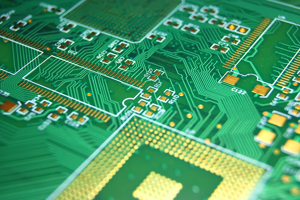
![]()
RIGID PCB CAPABILITIES
| FEATURE | STANDARD | ADVANCED |
| Min Layer Count | 1 | 1 |
| Max Layer Count | 30 | 48 |
| Min Board Thickness | .010” (.254 mm) | .005” (.127 mm) |
| Max Board Thickness | .250” (6.35 mm) | .370” (9.40 mm) |
| Min Core Thickness | .004” (.102 mm) | .002” (.051 mm) |
| Min Dielectric | .004” (.102 mm) | .003” (.076 mm) |
| Min Starting Copper Foil Weight | 9 microns | 9 microns |
| Max Finished Copper Thickness (O/L) | 4 oz (118 ml) | 6 oz (177 ml) |
| Max Finished Copper Thickness (I/L) | 4 oz (118 ml) | 4 oz (118 ml) |
| Min Panel Size | 12” x 18” (30 x 46 cm) | 12” x 18” (30 x 46 cm) |
| Max Panel Size | 18” x 24” (46 x 61 cm) | 23” x 32” (57 x 82 cm) |
| Smallest Mechanical Drill Diameter | .0059” (.150 mm) | .0059” (.150 mm) |
| Smallest Laser Drill Diameter | .005″ (.127 mm) | .004″ (.102 mm) |
| Min Finished Hole Size | .004” (.102 mm) | .002” (.051 mm) |
| Max Through Hole Aspect Ratio (depending on board thickness and finish hole) | 10:01 | 10:01 |
| Max Laser Via Aspect Ratio | .75:1 | .75:1 |
| Blind Via Finished Hole Size | .004” (.102 mm) | Plated Shut |
| Buried Via Finished Hole Size | .004” (.102 mm) | .002” (.051 mm) |
| Min Trace and Space | .004” (.102 mm) | .003” (.076 mm) |
| Line/Space Inner Layer | 3mil/3mil (HalfOZ) | 2 mil/2 mil (HalfOZ) |
| 4mil/4mil (1OZ) | 3 mil/3 mil (1OZ) | |
| Line/Space Outer Layer | 4mil/4mil | 3 mil/3 mil |
| 4.5mil/4.5mil | 4mil/4mil | |
| Min Pad Size for Test | .005” (.127 mm) | .005” (.127 mm) |
| Process Pad Diameter | D + .012” (.305 mm) | D + .008” (.203 mm) (tangency) |
| (1-mil (.025-mm) annular ring) | ||
| BGA Back Drill | Stub=7+/-5milwith 100mil depth | Stub=6+/-4milwith 100mil depth |
| BD2M=5mil | BD2M=4.8mil | |
| 0.30mm Via in BGAwithout trace | 1mm BGAwith two trace | |
| Stacked Vias | Yes | Yes |
| Min Wire Bond Pad Size | > .006” (.152 mm) | .004” (.102 mm) |
| Controlled Impedance Tolerance | 10% | 5% |
| Solder Mask Registration | .002” (.051 mm) | .001” (.025 mm) |
| Solder Mask Feature Tolerance | .0015” (.038 mm) | .001” (.025 mm) |
| Solder Mask Min Dam Size (based on green soldermask color) | .005” (.127 mm) | .004” (.102 mm) |
| Min Diameter Route Cutter Available | .024” (.610 mm) | .021” (.533 mm) |
| Routed Part Size Tolerance | .005” (.127 mm) | .003” (.076 mm) |
| Laser Hole Location Tolerance | .0005” (.013 mm) | .0005” (.013 mm) |
| Laser Routed Part Size Tolerance (< .032” thick) | .002” (.051 mm) | .002” (.051 mm) |
| Bow and Twist Tolerance | Per IPC spec | Per IPC spec |
| Thickness Tolerance (based on board thickness) | 10% | 5% |
| Sequential Laminations | 3 or less lamination cycles | 4 lamination cycles |
| Buried Vias | Yes | Yes |
| Blind Vias | Yes | Yes |
| Conductive Filled Vias | Yes | Yes |
| Non Conductive Filled Vias | Yes | Yes |
| Surface Finishes | OSP, ENIG, Immersion Tin, ImmersionAg, HASL, LF-HASL, Golden Finger ,Selective ENIG+OSP,Selective Hard Gold, Soft Gold, Flash Gold | |
| Materials | Std. FR4, High Tg FR4, TUC, Shengyi, Iteq, Panasonic, Ventec, Nelco, Isola, Rogers, Dupont, Arlon | |
| Solder Mask | Green, Black, Red, Clear, White | |
| Standards | IPC6012 Class 1, 2, 3 | |
![]()
Applications for PCBs
Printed Circuit Boards are widely used in various applications across many industries due to their durability, stability, and reliability. Some common applications of rigid PCBs include:
- Electronics and Consumer Devices: Rigid PCBs are the backbone of virtually all electronic devices, from smartphones and laptops to televisions and home appliances. They provide the necessary connections for components and ensure proper functionality.
- Industrial Equipment: Rigid PCBs are extensively used in industrial machinery, control systems, and automation equipment to facilitate precise control and data processing.
- Automotive Electronics: Modern vehicles rely on rigid PCBs for engine control units (ECUs), infotainment systems, safety features, and navigation systems, enhancing vehicle performance and safety.
- Medical Devices: Medical equipment, such as MRI machines, X-ray devices, and pacemakers, depend on rigid PCBs to ensure accurate diagnostics and treatment.
- Telecommunications: Rigid PCBs play a vital role in the infrastructure of the telecommunications industry, supporting the transmission and reception of data and voice signals.
- Lighting Systems: LED lighting systems utilize rigid PCBs for power distribution and control, contributing to energy efficiency.
These are just a few examples, as rigid PCBs have applications in various industries where the need for reliable and stable electrical connections and circuitry is essential. Their versatility and adaptability make them a cornerstone of modern technology and innovation.

![]()
Get A Quote
Whether you need a basic single-layer circuit board, or a complex 30-layer PCB using exotic metals, we can provide an instant quote and deliver your boards in as fast as 3 days, depending on technology.
Send us your Gerber files and drawings, or provide us with the following information for an immediate quote to get your project started.
| Feature | Industry Standard |
| Part Number (for easy tracking) | |
| Board Size | Rectangular |
| Number of Layers | 1-30 |
| Overall Thickness Required | .062” |
| Material Required | FR4 |
| Copper Weight | External 1oz/Internal 1oz |
| Minimum Trace/Space | .005/.005 |
| Solder Mask Color | LPI Green |
| Silkscreen Color | White |
| Routing | Panelized with V-cut/tabs or Single |
| Quantity Needed | >2 |
| Lead Time Required | 3 days -4 weeks |